VRoom! blog - Building on AWS
19 Dec 2021Introduction
I started doing VLSI design in the early ’90s building graphics accelerators at 2um and later in the decade building CPUs at 1.8u-0.5u - gates and pins were expensive - we once bet the company on the viability of a 208 pin plastic package, something that paid off magnificently.
I started this project with the vague idea of “what happens if I throw a lot of gates at it?” - my original planned development platform was a board off of Aliexpress a lot like this one an Xylinx Kinetix 420 based board with embedded DRAM - my plan was to wire an SD card socket to it and used the internal USB to serial hardware to boot linux.
When I first compiled up VRoom! for it I had a slight problem …. the design was 50% too big! oops ….
So I went around looking for bigger targets ….
AWS’s FPGA Instances
AWS provides an FPGA based service based on Xilinx’s Ultrascale VU9Ps - these are much larger FPGAs, just what the doctor ordered. The F instances seem to be aimed at high frequency traders - we’re small fry in comparison. They are based on a PCIE board in an Intel based CPU - we assume they actually put 4 boards into each CPU and sell the minimum as a virtual instance with 8 virtual cores and a physical FPGA board. This is the F1 instance that we use for development.
The AWS F instances each include a VU9P, 4 sets of DDR4 (we use one), and several PCIEs to the host CPU (we use one simple one).
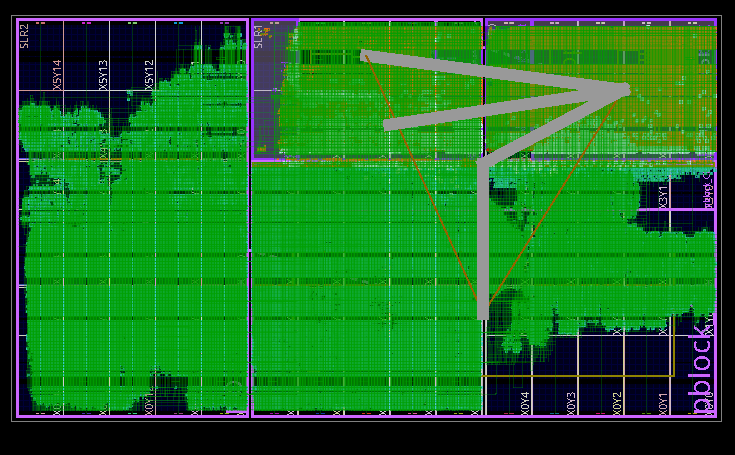
The VU9P is an interesting beast it seems to actually be a sandwich of 3 dies, with ~1500 wires between the middle die and the upper die and ~1500 wires between the middle die and the lower die. These wires make the thing possible but they’re also a problem, firstly they are potentially a scarce routing resource (not for us yet), and secondly they are slow - for speed Xilinx recommend that one carefully pipe all the die crossings (ie a flop on either side). We’ve decided to not do that, as it would mean messing with a design where we’re actually trying to carefully debug the actual pipelining for a real CPU. Rather than have this reality intrude on our design we’ve had to reduce our target clock from 100MHz to 25MHz currently most critical paths have several die crossings.

The above image shows a recent layout plot - you can see the three dies. The upper 25% on the center and right hand side dies is AWS’s “shell” a built in interface to the host CPU and one DDR4 controller. There is now a smaller shell available which we may switch to soon that removes a whole lot of functionality that we don’t need, and gives us ~10% more gates (but sadly in the wrong places).
Development is done on an AWS FPGA development instance, you don’t need to pay for a Vivado license if you do your development on AWS. The actual build environment, documentation (and the shell) is available on github.
Build time is very variable, our big problem is congestion (timing issues come from that) and builds can take any time from 10-20 hours and don’t always succeed. We’ve had to drop the sizes of out I/D caches by 50% and our BTC by 8x to make this work.
AWS don’t want us to trash their hardware so after you’ve completed building a new design you have to submit it for testing - they do a bunch of things presumably looking for over current and over temp issues (we haven’t had one rejected yet). This takes about an hour.
F1 instances cost ~US$1.50/hour to use, the build systems about US$1/hour.
Chip Architecture
AWS provide their “shell”, a fixed, pre-laid out interface - you can see it in this block diagram as “AWS support”:
The shell provides AXI interfaces looking inwards (our DRAM controller is a master, our disk/UART are clients).
We’ve added a simple UART, dumb fake disk controller (really just a 256-byte FIFO) to the shell, and a register that allows us to reset the VROOM!. These simple devices are made visible on the PCIE as registers and mapped into a user space linux app running on the host Intel CPU.
The VROOM! is instanced with a minimal number of connections (the above devices, DRAM and clocks). It is essentially the same top level we use in verilog simulation (from chip.sv down, one CPU and one set of IO devices).
Software
The Linux user space software is a thread that maps the PCIE register space and then pulls the CPU out of reset. It then loops reading from the UART and ‘disk’ registers, if it finds a disk request it provides data from one of two sources (an OpenSBI/Uboot image or a linux file system image), if it finds incoming uart data it wakes a text display thread to print it on the console. A third thread reads data from the console and puts it into the uart to send when space is available.
Software release
We haven’t included the AWS interface code in the current VROOM! source release, partly because we don’t want to confuse it with the real thing we’re trying to build. But also because it’s mostly embedded in code that is AWS’s IP (the shell API is one big verilog module that one needs to embed one’s own IP) - there are no secrets on our part, we’re happy to share if anyone is interested.
Next time: (probably after Xmas) Virtual Memory
